
Hi Marek/Fabio,
I think there's an error in code setting up the CPU clock in the SPL for the i.MX28. When instruction stepping through mx28_power_clock2pll in spl_power_init.c, the processor drops dead right after PLL bypass has been disabled.
The i.MX28 reference manual (pag 116) states that the JTAG clock is derived from the CPU clock and that the JTAG tap will stop working if CPU clock is stalled, too low or disabled. I figured that disabling PLL bypass would temporarilly cause an irregular clock, throwing off the probe, even in adaptive clocking mode. Three different probes later, I know it is not.
Freescal tech support said it may be related to a non ARM specification shortcut in the clock tree, but that's not causing the problem either.
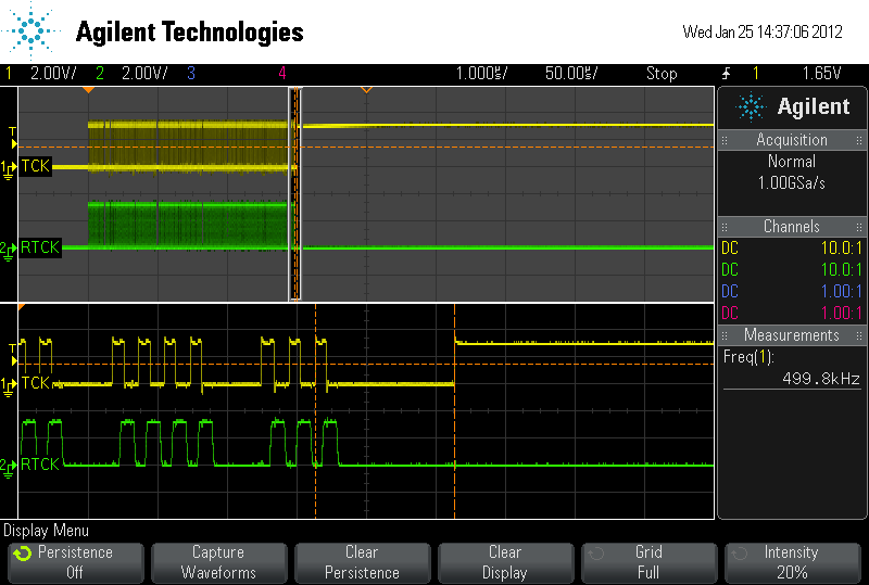
I succeeded in reproducing the problem using only my JTAG probe (Abatron BDI300) on adaptive clocking. Below the transcript of the probe's command line interface: 926E>reset ... 926E>md 0x80040000 1 80040000 : 0x00000000 0 .... 926E>mm 0x80040000 0x00020000 926E>md 0x80040000 1 80040000 : 0x00020000 131072 .... 926E> 926E>md 0x800401d0 1 800401d0 : 0x000441ff 279039 .A.. 926E>mm 0x800401d0 0x000041ff 926E>md 0x800401d0 1 After the last command, both mx28evk board and JTAG probe hang. The last JTAG transaction, caused by the last 'mm'-command, is shown on attachement 'TCK-RTCK, Adaptive, No Frac0.png'. This picture shows that the transaction the probe is raising TCK, but the target is no longer following it, as it's supposed to do.
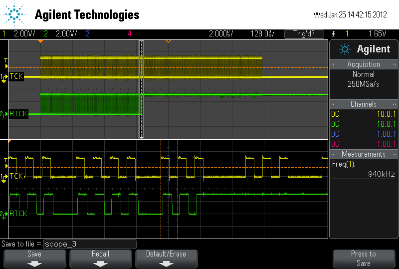
When configuring the probe at a fixed clock of 1MHz, the same sequence no longer hangs up the probe, but just hangs up the target: 926E>reset ... 926E>md 0x80040000 1 80040000 : 0x00000000 0 .... 926E>mm 0x80040000 0x00020000 926E>md 0x80040000 1 80040000 : 0x00020000 131072 .... 926E> 926E>md 0x800401d0 1 800401d0 : 0x000441ff 279039 .A.. 926E>mm 0x800401d0 0x000041ff 926E>md 0x80040000 1 80040000 : 0xffffffff -1 .... The last read-back is obviously a bogus value. The last JTAG transaction, caused by the last 'mm'-command, is shown on attachement 'TCK-RTCK, 1MHz, No Frac0.png'. This picture shows that half-way the transaction the stops outputting RTCK, while the probe continues on it's fixed clock.
I think the cause of this problem is that PLL bypass is disabled - using PLL0 as CPU clock source instead of it's reference xtal - while CPU clock gating on PLL0 is still enabled. Now I don't fully understand why this problem only occurs when instruction-stepping the code, and not under normal operating conditions. It may be related to delay, because some time later mx28_mem_init in spl_mem_init.c does disable CPU clock gating on PLL0.
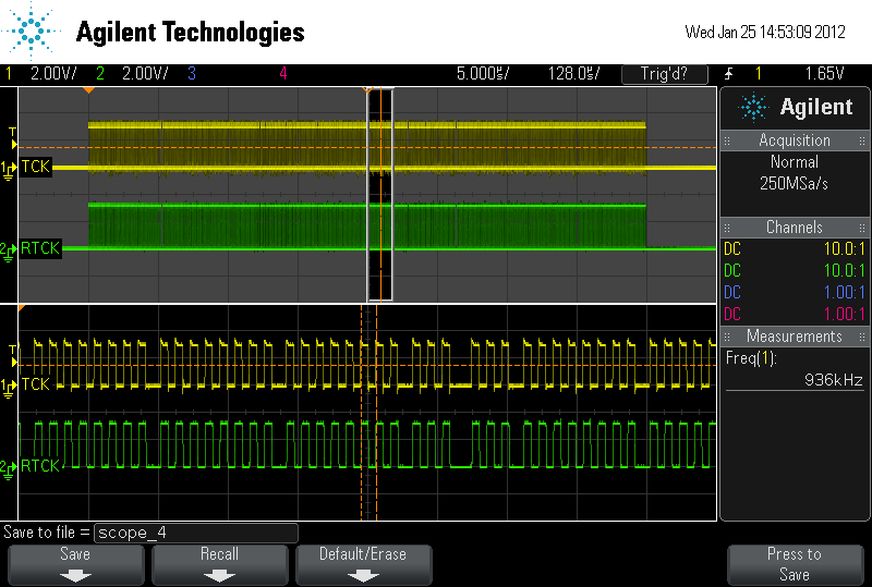
I have tested this by modifying the sequence above by inserting commands to disable CPU clock gating: 926E>reset ... 926E>md 0x80040000 1 80040000 : 0x00000000 0 .... 926E>mm 0x80040000 0x00020000 926E>md 0x80040000 1 80040000 : 0x00020000 131072 .... 926E> 926E>md 0x800401b0 1 800401b0 : 0x92929292 -1835887982 .... 926E>mm 0x800401b0 0x12525513 926E>md 0x800401b0 1 800401b0 : 0x52521513 1381111059 ..RR 926E> 926E>md 0x800401d0 1 800401d0 : 0x000441ff 279039 .A.. 926E>mm 0x800401d0 0x000041ff 926E>md 0x800401d0 1 800401d0 : 0x000041ff 16895 .A.. After this sequence, both probe and board are still fully responsive. Even the written value can be read back successfully. Attachement 'TCK-RTCK, Adaptive, Frac0.png' shows the JTAG transaction, caused by the last 'mm'-command. The zoomed section at the bottom shows how the clock frequency increases half-way the command.
The sequence above changes more to the clkctrl_frac0 register than just disabling CPU clock gating, but I have repeated this sequence writing a value of 0x92929212 (over a power-up default of 0x92929292) and that works just the same.
Shouldn't we configure clkctrl_frac0 - or at least disable CPU clock gating - before disabling PLL bypass?
Cheers,
Robert.